6
Siltronic AG celebrates the inauguration of the new fab in Singapore

Siltronic AG celebrates the inauguration of the new fab in Singapore


Siltronic AG celebrates the inauguration of the new fab in Singapore

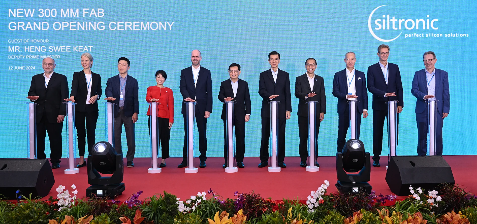
[From left to right] Dr. Rüdiger Schmolke, CTO of Siltronic; Claudia Schmitt, CFO of Siltronic; Dr. Kim Yong Kwan, Siltronic Silicon Wafer Board of Directors Member; Jacqueline Poh, EDB Managing Director; Dr. Michael Heckmeier, CEO of Siltronic; Heng Swee Keat, Deputy Prime Minister; Niew Bock Cheng, Siltronic Singapore Site President; Tan Boon Khai, CEO of JTC; Dr. Tobias Ohler, Chairman of the Supervisory Board of Siltronic; Klaus Buchwald, COO of Siltronic; Bernhard Schmidt, Project leader of new fab and Siltronic Senior VP Engineering/Strategic Procurement. Photo credit: Siltronic AG (photo credit: Siltronic AG)

This press release was issued by Siltronic AG.
 

Today marks a milestone in the history of Siltronic AG: After more than 500 construction days and roughly 23 million working hours, Siltronic inaugurated one of the world’s most advanced wafer fabs. The inauguration of the new production facility, which is one of the most modern and cost-efficient of its kind, took place today.

The highly automated fab at JTC’s Tampines Wafer Fab Park was officially opened in the presence of around 150 guests, including numerous high-ranking representatives of the Singaporean government, customers and suppliers. Singapore’s Deputy Prime Minister Heng Swee Keat was the Guest of Honour to grace the occasion. The fab was commissioned at the beginning of 2024 and will now be ramped to full capacity over several years.
"With our new fab, we will accompany the future growth of the wafer industry for many years to come and take Siltronic to a new level. What the entire team, including all business partners, has achieved is a masterpiece, and I would like to thank everyone for their outstanding contribution."

Dr. Michael Heckmeier

CEO

Siltronic AG

“We are proud of our long-standing partnership with Siltronic. As one of top 5 global wafer suppliers, Siltronic’s new fab is a significant expansion that not only supplies to Singapore’s semiconductor industry but also strengthens the resilience of the global semiconductor supply chain. This investment will create good jobs and further grow the existing collaboration that Siltronic has with local suppliers in automation and precision components.”

Jacqueline Poh

Managing Director

EDB

The success story of Siltronic in Singapore began in 1997 with the founding of Siltronic Singapore Pte. Ltd. in JTC’s Tampines Wafer Fab Park. The first 200 mm wafers were produced as early as 1999. This was followed in 2006 by the establishment of a joint venture with Samsung and the start of construction of the first 300 mm fab, from which the first wafers were delivered to customers in 2008. The foundation stone for the second 300 mm fab was laid in 2021, and it was officially opened today. Singapore is Siltronic's largest production site.

Today's inauguration of the state-of-the-art wafer fab in Singapore is not only the largest investment in Siltronic's history, but also a milestone of which Siltronic is extremely proud. With its high level of automation and impressive efficiency, the fab sets new standards in our industry and strengthens Siltronic’s position as one of the world's leading wafer manufacturers.

Contact Us Icon
Reach out to us for information on how we can facilitate your investment journey
Subscribe Icon
The latest business insights and news delivered to your inbox
Subscribe now