Chips, wafers, and semiconductors – these terms are often used interchangeably, but they do not technically refer to the same thing.
Semiconductor: A material that is able to act as both a conductor and an insulator of electricity. Examples include silicon, germanium and sapphire. Silicon is particularly popular for use in manufacturing, partly due to its abundance; it is the second-most abundant element on Earth, after oxygen.
Wafer: A thin circular slice of semiconductor material that forms the base of a chip. The silicon used to make wafers needs to be 99.9999 per cent pure, a level known as “six nines”. Standard wafers are 300 millimetres in diameter. Wafers with a larger diameter are considered more cost-effective, as more chips can be cut per unit of area, due to how they fit within a circle.
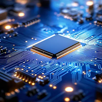
Integrated circuit (IC): Also known as microchip or chip, this is a self-contained device; an assembly of electronic circuits on a small piece of silicon. ICs contain components such as resistors and up to billions of transistors, which are semiconductors that amplify or switch electrical signals.
From wafer to chip
First, electronic circuits are fabricated on wafers. Patterns of ICs are drawn onto a wafer using beams of light, in a process known as photolithography or UV lithography. This is followed by etching, in which chemicals are used to selectively remove unwanted layers from the wafer’s surface, leaving behind the desired pattern.
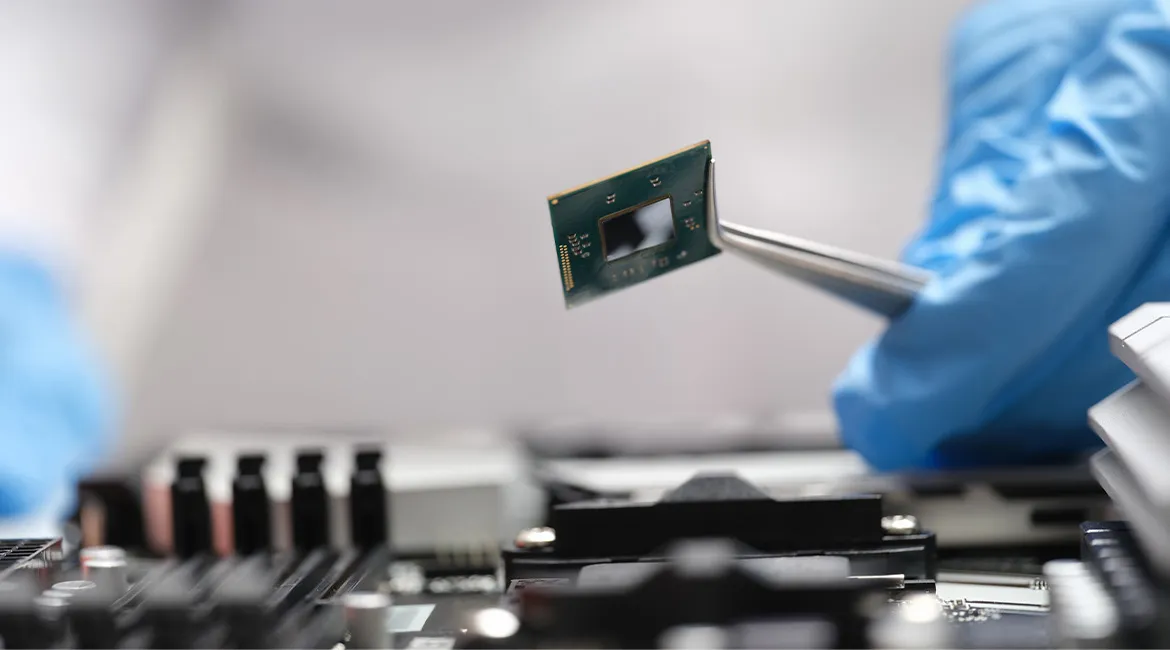
The wafer is then cut into small pieces. Each piece, known as a die, forms the basis of an IC chip.
Process node: Also known as technology node, these are measured in nanometres (nm). Historically, the measurement referred to the size of transistors on the chip. However, the number has since become arbitrary, and simply conveys how advanced a chip is compared to previous ones.
A smaller number implies that a chip has a greater density of transistors and is thus faster. Mature-node chips, also known as legacy chips, use process nodes of 28 nm or more. Leading-edge artificial intelligence chips typically have process nodes of 7 nm or less.
Packaging: This refers to casings of metal, ceramic, glass or plastic, which protect IC chips and connect them to other chips or a device’s circuit board.