6
US chip gear giant Applied Materials to double Singapore manufacturing, R&D and headcount

US chip gear giant Applied Materials to double Singapore manufacturing, R&D and headcount


Applied Materials CEO Gary Dickerson said the company will have to collaborate with more partners to speed up innovation in packing technologies.

Applied Materials CEO Gary Dickerson said the company will have to collaborate with more partners to speed up innovation in packing technologies.

Applied Materials (AM), one of the world’s top suppliers of machines that make semiconductors, plans to double its Singapore manufacturing capacity, headcount, and research activities in the coming years.

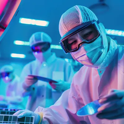
The US company will soon announce the expansion of one of its innovation centres here that focuses on advanced packaging of semiconductors – the integration of a multitude of components into a single package to enhance performance and power efficiency without a significant increase in the size and cost of the product.

AM is already one of the largest employers and contributors in the output of Singapore’s semiconductor equipment industry, which has a global market share of 20 per cent.

Singapore is also its Southeast Asia headquarters.

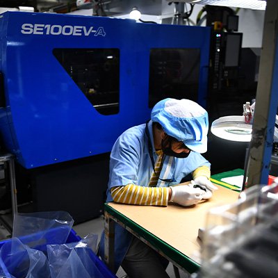
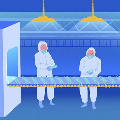
Earlier this year, the company’s new S$600 million plant in Tampines Industrial Crescent started operations. The new plant will employ 1,000 staff once it is fully functional.

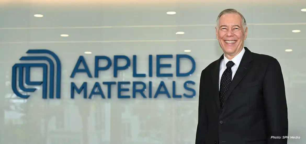
“We have a significant manufacturing, supply chain and R&D footprint here in Singapore,” said Mr Gary Dickerson, president and chief executive of the Santa Clara, California-based company.

“We have over 2,500 employees here in Singapore today, and I believe there is a great opportunity for us to more than double the size of Applied Materials and create many great jobs here,” he told The Straits Times in an interview at the company’s office in Changi North Industrial Estate.


The Advanced Packaging Development Centre was established in 2011 as a joint lab partnership with the Institute of Microelectronics (IME), a research institute of Singapore’s Agency for Science, Technology and Research (A*Star).

Since then, AM and IME together have invested about US$500 million (S$677 million) in upgrading and expanding the lab at Science Park II.

According to A*Star, the lab created over 100 high-value jobs for researchers, scientists, and engineers between 2011 and 2021.

“Advanced packaging is an incredibly important innovation for energy-efficient computing,” said Mr Dickerson, who on 11 June received the Public Service Star (Distinguished Friends of Singapore) award from President Tharman Shanmugaratnam at the Istana.

“So, whether it is in edge computing... or in high-performance computing for an AI (artificial intelligence) data centre, energy consumption is going higher and higher, and those data centres are becoming hotter and hotter.”

Hence, packaging technologies will see significant innovation, he said.

Mr Dickerson said while AM has the broadest portfolio of packaging technologies, the company will have to collaborate with more partners to speed up innovation in this area.

Singapore, with an established innovation platform and diverse ecosystem, is the perfect place to co-innovate, he added.


Experts believe advanced multi-chip packaging will be an imperative for key applications such as mobile devices, automotive computing and generative AI.

Boston Consulting Group in a May 2024 research note said value creation is migrating towards companies that can design and integrate complex, system-level chip solutions using concepts like advanced packaging.

“Merely making individual components will rapidly lose lustre, replaced by collaborative efforts that bring together the best in design, packaging, and system integration to meet the demands of the market,” it said.

Mr Dickerson said innovation around new chip architecture, materials, and processes will transform the semiconductor industry in the coming years.

“I guarantee you that what you see today in the market will be obsolete in the next few years,” he said. “Here in Singapore, expanding that packaging innovation lab will be incredibly important for Applied Materials, for Singapore and for the world.”

Investing in innovative technologies will be key for Singapore to boost its global semiconductor market share, observers say.

The Republic not only accounts for one-fifth of the global semiconductor equipment market, it is also a hub for chip fabrication firms, or fabs, that command an 11 per cent global share.

However, the fabs here mainly produce mature node chips that are typically used in Internet of Things, communications, automotive, power and sensor devices – or Icaps, as defined by Applied Materials.

Chips that are 28 nanometre (nm) or bigger are called mature nodes and chips smaller than 28 nm are considered advanced nodes and pack more transistors and have been key to bringing generative AI to life.

However, Mr Dickerson said that while advanced chips are profoundly important, Icaps will continue to be in demand in other high-growth applications.

“We see Icaps demand as sustainable, as these customers are delivering enabling technology for large, global inflections that will play out over the next decade,” he said.

Experts estimate that a megawatt generated by solar or wind requires US$3,000 to US$4,000 of power chips in panels and turbines.

“So, Singapore actually is really well positioned. For growth in those markets is going to be significantly faster than people understand,” Mr Dickerson said.
 

Source: The Straits Times © SPH Media Limited. Permission required for reproduction.

Related Content

Subscribe Icon
The latest business insights and news delivered to your inbox