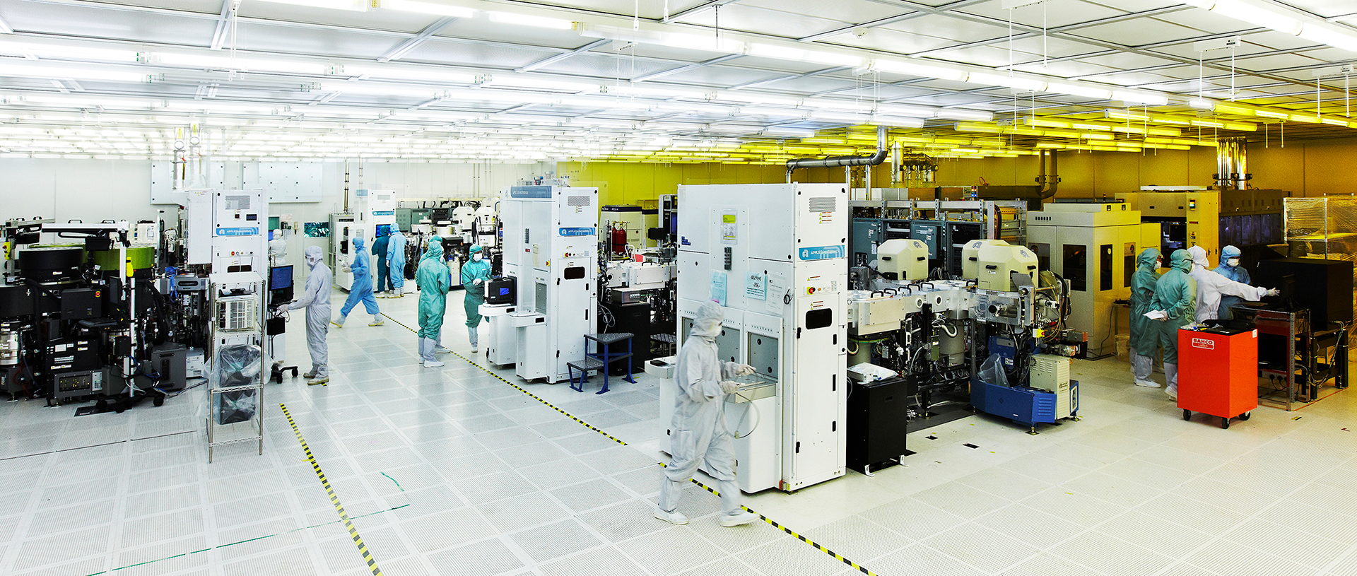
Today, the US company, which established its first Singapore office in 1991, has a total workforce of about 1,000 employees who are engaged in advanced semiconductor equipment manufacturing, research and product development, sales & service operations and other global corporate functions.
As part of its R&D efforts, the company has an ongoing research collaboration with A*STAR’s Institute of Microelectronics (IME). In 2012, an R&D joint lab was established with a combined investment of over US$100 million dedicated to research on advanced packaging equipment, process and device structures. As one of the most advanced and comprehensive facilities of its kind in the world, the lab features a 1,300 sqm Class 10 cleanroom with a full line of wafer processing and packaging equipment.
The lab leverages Applied Materials’ expertise in materials engineering and IME’s leading research capability in 3D integrated circuit packaging to develop technology that can enable smaller packages, lower power consumption and higher data bandwidth, which are advancements necessary to feed the global demand for mobile devices. The partnership has helped the Nasdaq-listed company develop cutting-edge technology that has been successfully implemented in several of its semiconductor equipment products.
The success of the partnership has led to an additional US$150 million in combined investment and an expanded lab facility. The lab now covers a total area of about 1,700 sqm with a team of close to 100 researchers, scientists and engineers working on leading-edge research areas like Fan-out Wafer Level Packaging – a key technology platform for system scaling and multi-die packaging to enable even smaller chips and devices with greater speed and functionality.


